
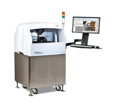
Brand:Bruker
Model:Dektak XTL
The new Dektak XTL™ stylus profiler provides extremely accurate, repeatable, and reproducible metrology for a wide range of applications. With its ability to accommodate samples up to 350mm x 350mm, this system finally brings legendary Dektak performance to 200mm and 300mm wafer manufacturing.
The Dektak XTL features a small footprint and integrated isolation with interlocking doors, making it ideal for today's demanding production floor environments. Its dual-camera architecture enables enhanced spatial awareness, and its high level of automation enhances manufacturing throughput. Bruker's exclusive Vision64 advanced production interface with optional pattern recognition makes data collection an intuitive and repeatable process, and minimizes operator-to-operator variability.
New software features make the Dektak XTL the most powerful, easiest to use stylus profiler available. The system utilizes Vision64 software that is fully compatible with Bruker’s optical profiler line. The Vision64 software enables unlimited measurement sites, 3D mapping, and highly customized characterization with hundreds of built-in analysis tools.
Also use Vision Microform software to measure shapes such as radius of curvature. Use pattern recognition to minimize operator error and enhance measurement location accuracy. Data collection and 2D and 3D analysis are in one software package with an intuitive flow. Each system comes with a Vision software license which can be installed on a separate PC with Windows 7 OS so data analysis and reports can be created at your desk.
With its unique combination of superior performance and ease of use the Dektak XTL is the new standard for industrial thin film deposition monitoring in touch-panel, solar, flat panel display and semiconductor industries for research and QA/QC.
Critical Results for Large-Format Applications
With its unique combination of superior performance and ease of use, the Dektak XTL is the new QA/QC and research standard for industrial thin film deposition monitoring in touch-panel, solar, flat panel display, and semiconductor industries.
Wafer Applications:
Step height for deposited thin films(metals, organics)
Step height for resists (soft film materials)
Etching rate determinations
Chemical mechanical polishing(erosion, dishing, bow)
Large Substrate Applications:
Printed circuit boards (bumps, step heights)
Window coatings
Wafer masks
Wafer chuck coatings
Polishing pads
Glass Substrate and Display Applications:
AMOLEDs
Step height measurements for LCD R&D
Film thickness measurements for touch panels
Thin film measurements for solar coatings
Click to learn more product information.
Contact our application team immediately: 021-37018108, info@boyuesh.com
Tel:86-021-37018108
Fax:86-021-57656381
Email:info@boyuesh.com
Address:Room 301, 28 Songjiang Hi-tech park, 518 Xinzhuan Road, Songjiang District, Shanghai